 uogent®
Analysis / Electronics Manufacturing
Making Memory Resilience a Core Mission of Semicon 2.0
India can use the current pressure on conventional DRAM supply to establish a practical position in global memory manufacturing: first through assembly, module production, test and qualification, then through higher-value packaging, components and, if commercial conditions support it, front-end production.
The memory shortage is not only a constraint on electronics and compute markets. It also shows where capacity is scarce and where additional qualified suppliers could be useful. For India, the near-term opportunity is not to begin with high-bandwidth memory, or HBM. It is to expand from current back-end operations into mainstream DRAM products that global customers can qualify and purchase at scale.
“RAM” is the familiar label. The industrial constraint sits mainly in the DRAM family. Conventional DRAM is used as working memory in servers, personal computers, networking equipment and many long-lifecycle systems. HBM is a specialised form of DRAM that is stacked and integrated close to AI accelerators to deliver much higher bandwidth. The products are different, but they compete for some of the same investment, cleanroom capacity, specialist skills, packaging capability and management attention.
Mainstream or long-lifecycle memory is not lower-quality memory. The terms refer to product architecture, performance, form factor and service life. A DDR4 module used in industrial equipment and an HBM stack used beside an accelerator serve different requirements and follow different manufacturing and qualification paths.
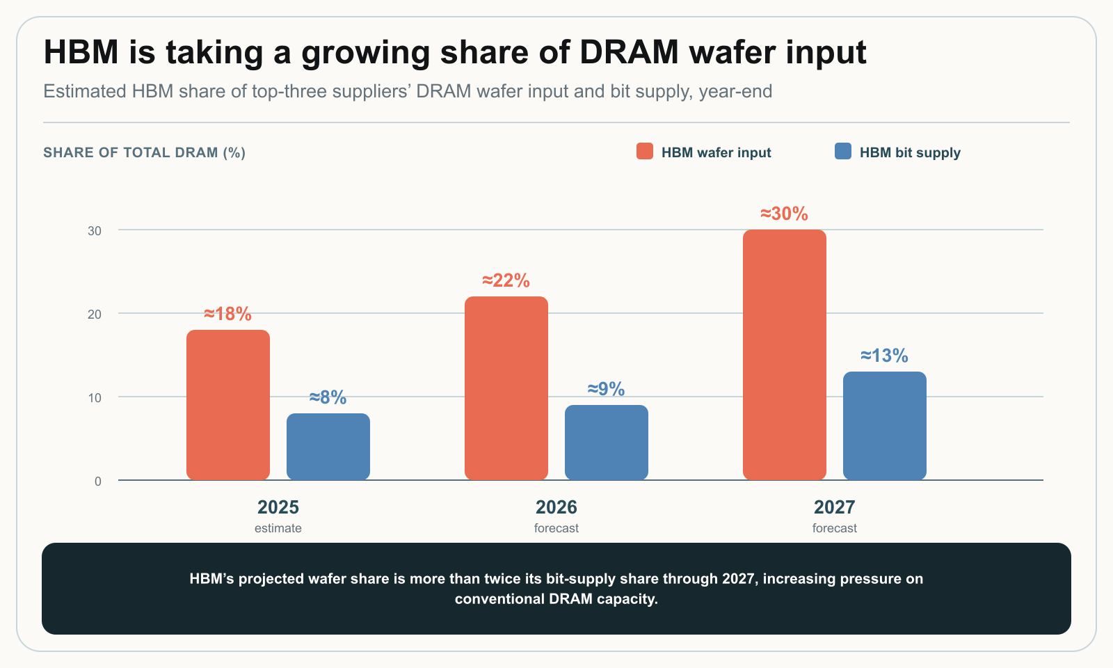
Their two products interact upstream. HBM absorbs a growing share of DRAM wafer input and attracts capital, engineering attention and advanced packaging capacity. Micron’s June 2026 results said the increasing amount of wafer input required for each new HBM generation places additional pressure on non-HBM supply.
India does not yet have a commercial DRAM wafer fab. It does, however, have an operating memory assembly and test base. Micron’s Sanand facility converts imported DRAM and NAND wafers into finished products, has begun commercial production and made its first shipment of India-made memory modules to Dell, according to the company’s facility-opening announcement.
That operating base provides a practical starting point. The objective for Semicon 2.0 should be to make Indian facilities qualified, reliable and cost-competitive across a wider range of conventional memory products, then use the resulting production experience to move into more complex packaging and, over time, selected front-end manufacturing.
Why the pressure extends beyond HBM
Memory markets have always moved in cycles. Producers add capacity, demand changes, inventories rise or fall and prices respond. The present squeeze has a more structural element because AI systems require large quantities of HBM while servers, personal computers, vehicles and industrial equipment continue to require conventional DRAM.
TrendForce estimated in June 2026 that HBM would absorb 22% of total DRAM wafer input among the three largest suppliers by the end of 2026 and 30% by the end of 2027, while supplying only 9% and 13% of DRAM bits. Its forecast points to increasing pressure on the wafer capacity available for conventional products.
Micron identifies several reasons why supply cannot respond quickly: long fab-construction lead times, shortages in critical construction trades, permitting complexity, energy constraints and smaller bit gains from each new process generation. Its June 2026 outlook expected supply to improve gradually in 2028 but did not identify when it would catch demand.
Other producers describe similar conditions. Samsung’s first-quarter 2026 results linked record memory performance to limited supply and industry-wide price increases. SK hynix said customer demand exceeded supply capacity.
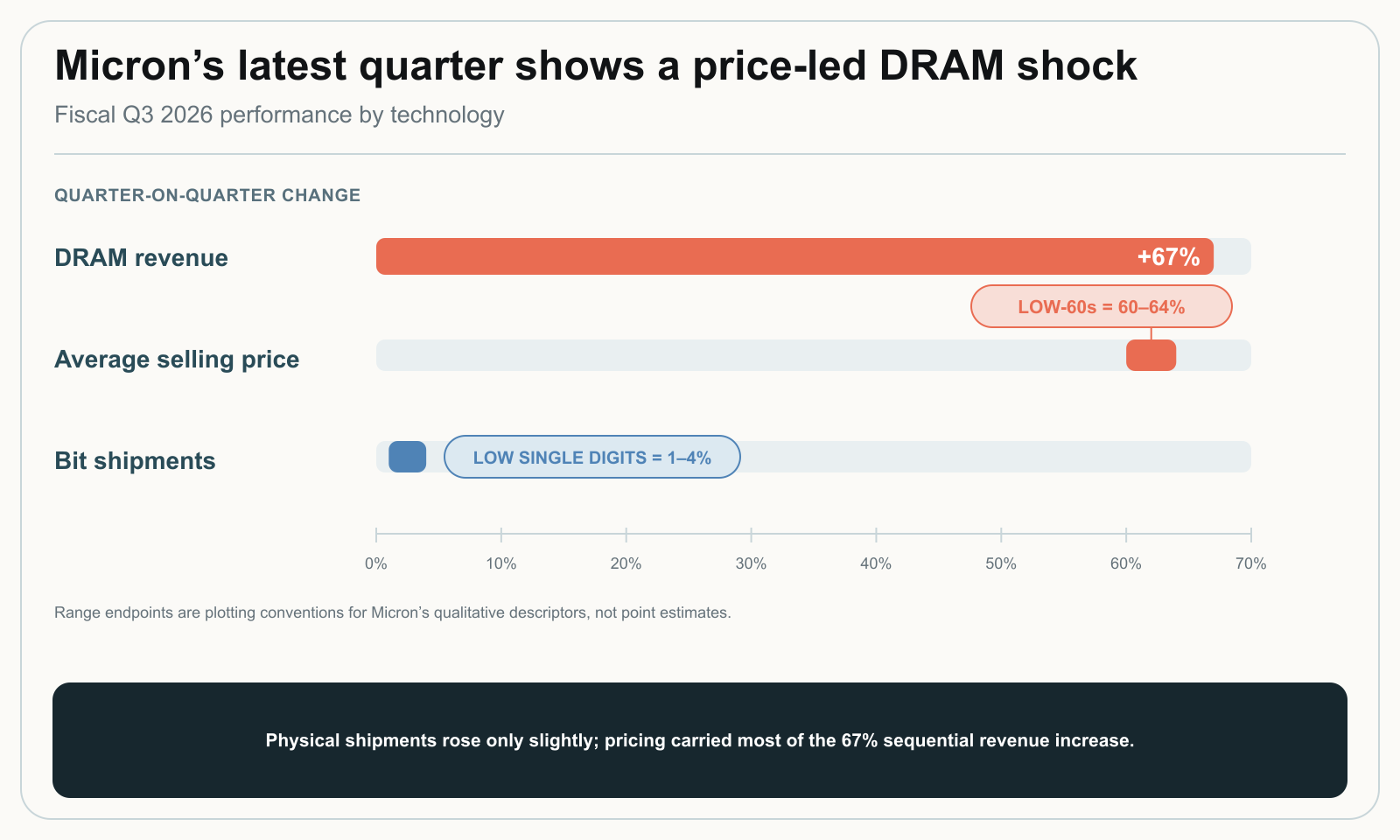
Prices show how quickly the imbalance is reaching the market. In Micron’s fiscal third quarter of 2026, DRAM revenue rose 67% from the previous quarter. Bit shipments increased only in the low-single digits, while average selling prices rose in the low-60% range, according to the company’s quarterly presentation.
The pressure on conventional DRAM does not mean ordinary module lines are simply being converted to HBM. HBM requires die stacking and advanced integration with logic devices, while a conventional DIMM is a replaceable board-level product. The common constraint is the allocation of wafer input, capital and specialist capacity across the broader memory portfolio.
This distinction defines the industrial opening for India. A shortage of DRAM wafers cannot be resolved by adding module assembly alone. However, tight supply increases the value of back-end operations that can convert available wafers and packaged devices into qualified finished products with high yield, predictable cycle times and reliable delivery to global customers.
It also increases the importance of long-lifecycle products. Micron is expanding 1-alpha DDR4 output in the United States for automotive, industrial, medical, aerospace and defence applications, illustrating that conventional memory remains commercially and strategically relevant alongside leading-edge products. The company’s May 2026 announcement describes the additional output as support for long-lifecycle customer requirements.
Enter through mainstream memory products
The memory value chain has several distinct stages: wafer fabrication; die packaging and test; module design and board assembly; electrical and reliability validation; and integration into a customer’s system. A country does not need to perform every stage on the first day to become part of the chain.
India’s most immediate route is through conventional assembly and test and through client, server and selected industrial memory modules. These products use established DRAM interfaces and serve large markets, but they still require precise manufacturing. A qualified supplier must control component traceability, board assembly, firmware configuration, signal integrity, thermal behaviour, electrical test and product reliability.
DDR5 illustrates how module production has become more technically demanding. The module includes active components such as a power-management integrated circuit and a serial-presence-detect hub in addition to DRAM packages and the printed circuit board, as described in Micron’s DDR5 module paper. This creates work in board design, component integration, programming, validation and test even when the DRAM die is fabricated abroad.
Imported wafers, dies or packaged DRAM can support the first phase in packaging, board assembly, test engineering, failure analysis and customer qualification. As qualified output and repeat orders grow, predictable demand for boards, substrates, sockets, burn-in hardware, fixtures, thermal materials and equipment services can make supplier co-location commercially viable.
Customer qualification is the threshold between local assembly and participation in the global supply chain. Customers require evidence that a product meets performance and reliability requirements over repeated production lots. Yield, defect rates, traceability, failure-analysis response and change control matter as much as installed capacity.
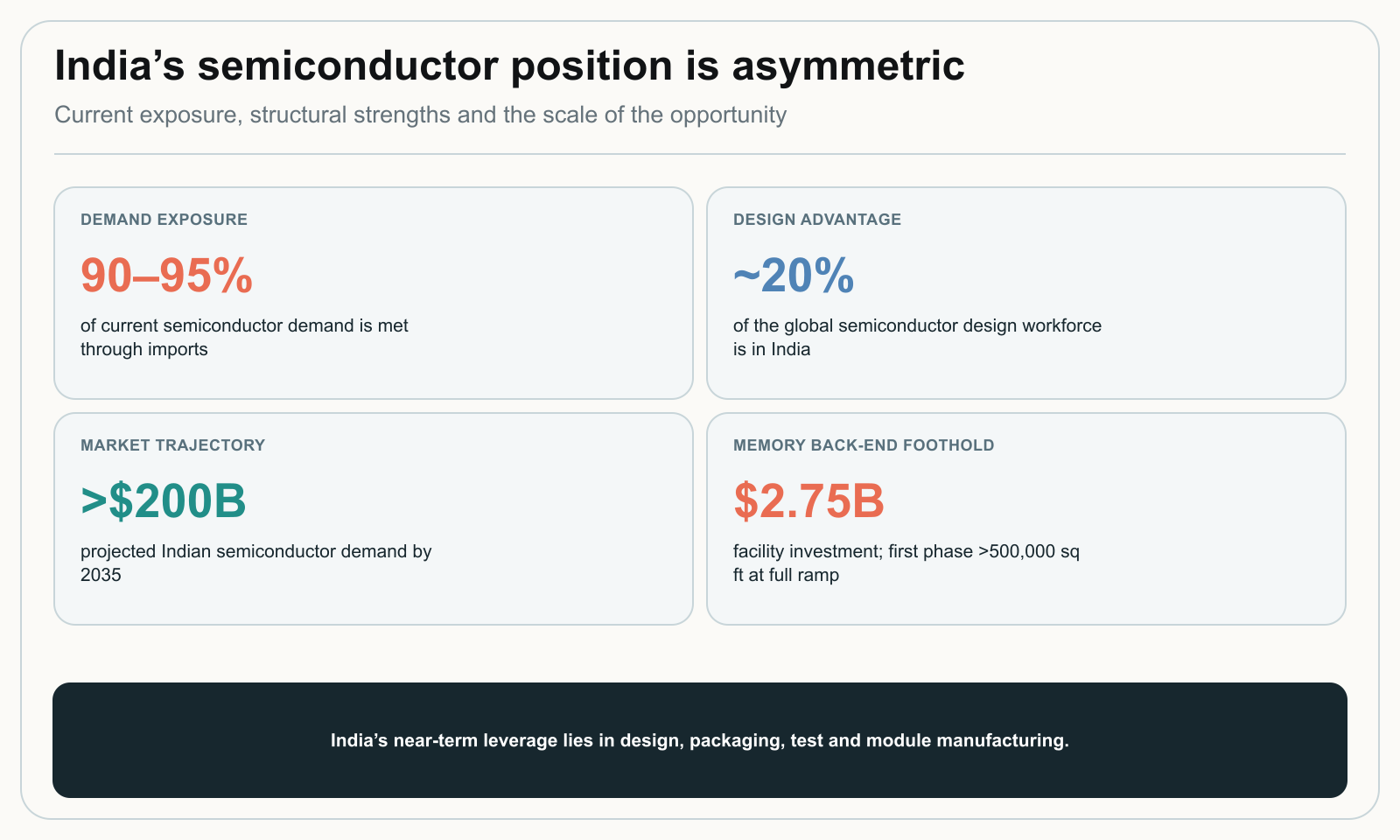
Micron’s Sanand operation shows that this route is already under way. The facility serves customers worldwide, and Micron describes its conventional assembly and test operations in India as a complement to advanced manufacturing and packaging investments elsewhere. At full ramp, the first phase is expected to exceed 500,000 square feet of cleanroom space, with output rising from tens of millions of assembled and tested chips in 2026 to hundreds of millions in 2027.
India’s domestic market can support production learning and initial qualification. Shared compute grew from 38,231 onboarded GPUs in March 2026 to more than 45,000 by late June. The Digital India update reported the June figure, while a separate government data-centre update placed national data-centre capacity at about 1,500 MW in 2025, four times its 2020 level.
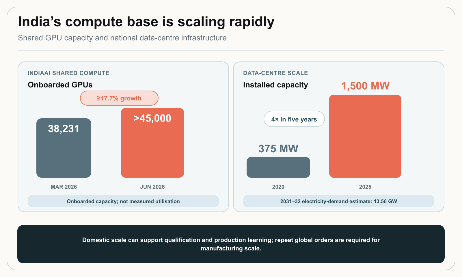
This demand is useful as an anchor market, but it is not sufficient by itself. Memory manufacturing achieves scale through repeat orders across several customers and end markets. The relevant test is whether products made in India enter global vendor lists, remain qualified across successive lots and generate export as well as domestic revenue.
Build on India’s operating base
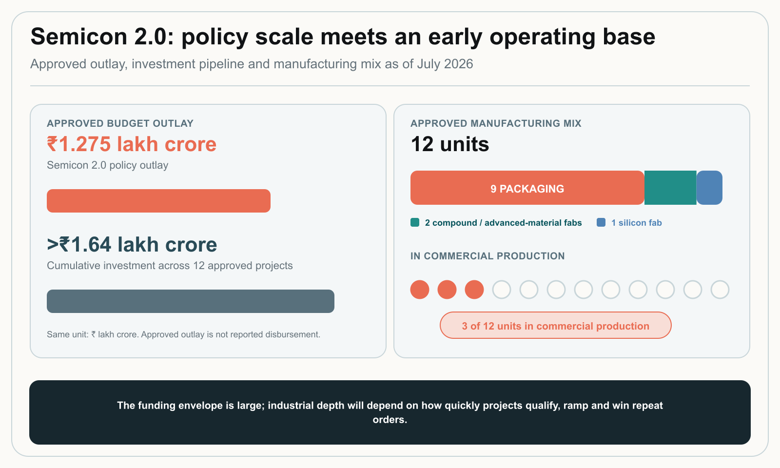
The Union Cabinet approved Semicon 2.0 in July 2026 with a budget outlay of ₹1,27,500 crore. The Cabinet approval covers design, equipment, materials, fabs, assembly and test, research and talent.
That scope is relevant to memory because competitiveness depends on an ecosystem rather than one plant. An assembly line needs qualified materials, reliable utilities, equipment service, test engineering, logistics and trained operators. A module business also needs board design, component sourcing, product engineering and access to customer qualification.
Under the first semiconductor mission, 12 projects representing more than ₹1.64 lakh crore in investment had been approved: one silicon fab, two compound or advanced-material facilities and nine packaging units. Three were in commercial production by July 2026, and the first silicon fab was scheduled for commissioning in 2028, according to the Semicon 2.0 approval.
Micron’s Sanand facility is the clearest memory-specific foothold. It takes advanced DRAM and NAND wafers produced elsewhere in Micron’s network and turns them into finished memory and storage products through assembly and test.
The facility represents about $2.75 billion in combined investment by Micron and its government partners. It is ISO 9001:2015 certified, has begun commercial production and has shipped India-made memory modules. These facts establish an operating reference point for workforce development, supplier qualification and production management.
They do not mean that India produces the underlying DRAM wafer. The distinction is important because each production stage should be measured separately. Packaging and test, module assembly, component manufacture and wafer fabrication require different equipment, skills, capital and technology partnerships.
The NITI Aayog semiconductor report estimates that imports meet 90–95% of current semiconductor demand and that the domestic market could exceed $200 billion by 2035. At the same time, India has about 20% of the global semiconductor design workforce.
The combination of design talent, electronics demand and an emerging back-end manufacturing base gives India a credible entry point. Current gaps include high-volume qualification, yield and reliability engineering, equipment support, experienced production managers and the supplier density associated with mature manufacturing clusters.
The appropriate sequence is to deepen the operating base before treating front-end wafer fabrication as the sole measure of progress.
Move from assembly capacity to qualified supply
The first capability to scale is conventional memory packaging and test. Facilities should be able to handle multiple package types, maintain high yields, trace material by lot and respond quickly when a customer identifies a failure. A line that passes an initial audit but cannot reproduce results at volume will not become a dependable global source.
The second capability is module productisation. India can build client, server and selected industrial modules using qualified DRAM devices, production-grade boards and tested firmware configurations. The product should be designed for a defined system and lifecycle rather than sold as undifferentiated capacity.
The third capability is shared validation infrastructure. Electrical, thermal, signal-integrity, burn-in, reliability and failure-analysis laboratories can reduce the cost and time required for module and packaging firms to qualify products. NITI Aayog’s roadmap proposes a national post-silicon validation laboratory and reliability infrastructure alongside advanced packaging.
The fourth outcome is a supplier network formed around sustained production. Boards, substrates, sockets, burn-in hardware, cleanroom services, metrology and equipment maintenance affect cost and production continuity. When plants move from pilot lots to repeat high-volume runs, predictable demand and shorter response times can justify nearby capacity.
The fifth capability is product and process engineering. Module design, firmware, controllers, interface intellectual property, power management, thermal design and manufacturing software can connect India’s design workforce to products made in India. This is where back-end manufacturing begins to generate proprietary know-how rather than only labour value.
Advanced packaging remains an important medium-term step. NITI Aayog proposes pilot lines for 2.5D and 3D integration, chiplets, hybrid bonding, advanced substrates and HBM-class integration, together with a post-silicon validation laboratory. The same roadmap calls for OSAT capacity aligned with both domestic fabs and global customers.
The progression should be based on demonstrated operating results. Conventional assembly and modules build volume discipline; customer qualification creates repeat demand; sustained utilisation makes nearby component and service capacity more commercially viable; advanced packaging adds more complex integration; and front-end production becomes more credible when there are experienced teams, customers and a supporting cluster.
Learn from peers, but use a staged route
Comparing semiconductor programmes only by announced spending can be misleading. A more useful comparison examines the operating tools around the funding: implementation capacity, industrial finance, tax treatment, research infrastructure, utilities and access to global customers.
The United States combines appropriations, lending capacity, tax credits and an advanced-packaging programme. Japan uses a dedicated implementation agency and specified-semiconductor support. South Korea combines finance, tax incentives, infrastructure support and next-generation stacked-memory research. The European Union combines public funding, research infrastructure and shortage monitoring. These instruments are summarised in NITI Aayog’s comparative policy analysis, with South Korea’s later measures described in its second-half 2026 work plan.
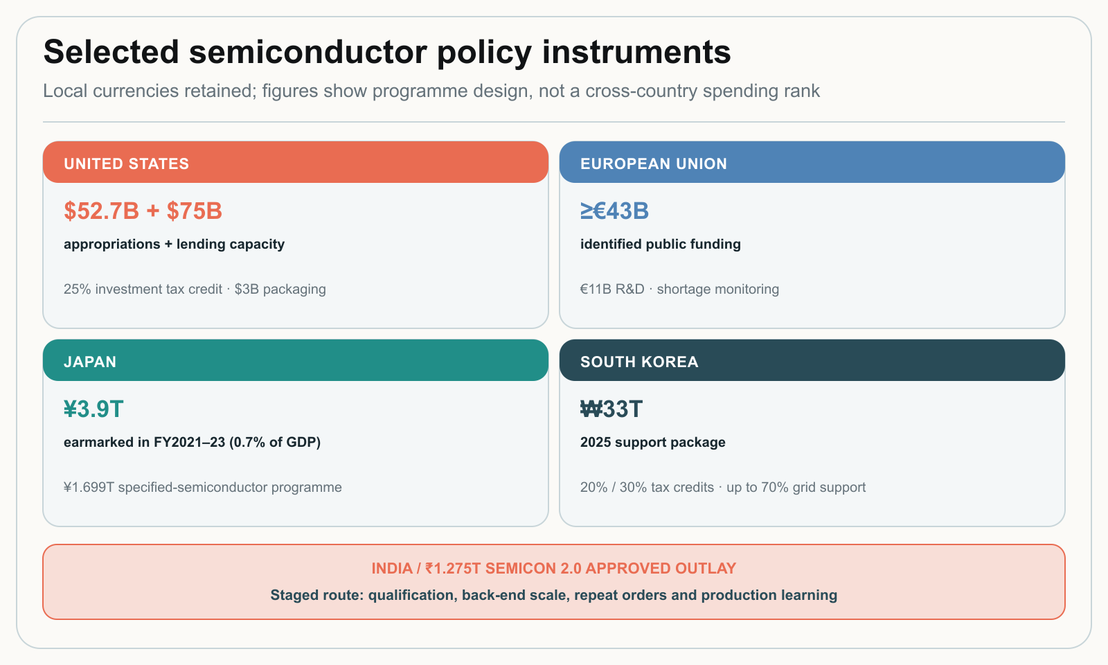
India begins from a different industrial position. Its strongest layers are design talent, domestic demand, software and a growing packaging base. Its weaker layers include memory-process technology, high-volume qualification, manufacturing leadership and the cluster density that usually accompanies sustained production volume.
A staged route reflects that starting point. In the near term, India can expand conventional memory assembly, test and module production. In the medium term, it can deepen reliability infrastructure, supporting components and advanced packaging. In the longer term, it can consider front-end memory production where a technology partner, customer base, utilities, equipment access and export economics are in place.
Each qualified product and repeat order adds demand for components and services. Rising utilisation and order visibility give suppliers a commercial reason to add capacity near the manufacturing base when lead-time, service and delivered-cost gains support it.
This sequence does not treat back-end manufacturing as a substitute for wafer fabrication. It treats back-end manufacturing as the operating base from which a broader memory cluster can develop.
Five actions for Semicon 2.0
Create a conventional-memory manufacturing window. Support qualified packaging, test and module capacity for client, server, networking and selected long-lifecycle products. Proposals should identify the target product family, source of DRAM devices, customer qualification plan, expected production volume and route to domestic and export markets.
Build shared memory qualification infrastructure. Establish laboratories for electrical validation, signal integrity, thermal testing, burn-in, reliability, failure analysis and traceability. Access should be available to module producers, packaging companies, design firms and their customers under clear confidentiality arrangements.
Scale through qualified demand. Move from pilot lots to repeat module and packaging runs, adding products and capacity as customers qualify them. Sustained utilisation and order visibility create the commercial basis for nearby component, service and logistics operations.
Evaluate projects by operating outcomes. Measure customer-qualified product families, yield, defect rates, cycle time, reliability performance, capacity utilisation, repeat orders, export shipments and successful production ramps. Approved investment and installed tools remain useful inputs, but they do not establish manufacturing capability by themselves.
Maintain a gated path to advanced packaging and front-end production. Advance HBM-class packaging pilots, post-silicon validation and workforce development in step with demonstrated demand and operating results. A front-end project becomes commercially credible when it has a technology partner, customer commitments, reliable utilities, equipment continuity and a plan for export competitiveness.
A small memory manufacturing programme office within the India Semiconductor Mission could coordinate these actions. Its role would be to define product segments, align common infrastructure, track customer qualification and report operating results that improve market visibility across the value chain.
Measure production capability
Semiconductor programmes often report approved investment, announced projects and installed tools. These figures show activity. They do not show whether a facility has become a regular source for customers.
By 2030, India should be able to report:
Qualified memory product families; annual packaged-device and module output; capacity utilisation; first-pass and final yield; defect and return rates; median failure-analysis time; number of global customer qualifications; on-time delivery; repeat-order revenue; and export share.
Supporting measures should include validated module designs; process changes that improve yield or cycle time; engineers with demonstrated packaging, test and reliability experience; the progression of products from pilot lots to sustained volume; supplier lead times; repeat component and service contracts; and new operating capacity near established manufacturing sites.
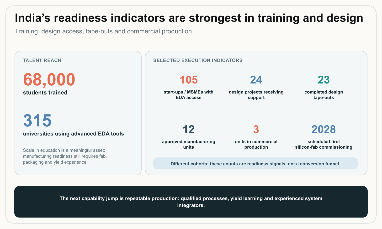
Current indicators show momentum, but also where the pipeline narrows. The Digital India update reports 315 universities using advanced design tools, about 68,000 students trained, 105 start-ups and small businesses with EDA access, 24 supported design projects and 23 completed tape-outs. The Semicon 2.0 approval reports that three of 12 approved manufacturing units were in commercial production by July 2026.
These figures describe different groups and should not be read as a single conversion funnel. Together, they indicate that India has a broad training and design base, while repeatable manufacturing and customer qualification are still developing.
The recommendation
Semicon 2.0 should treat memory resilience as an industrial-capability objective and make memory manufacturing a defined programme of work.
The current shortage creates a relevant market context. HBM is absorbing more DRAM wafer input and advanced packaging investment, while conventional DRAM remains necessary across servers, personal computers, networking, vehicles and industrial systems. Qualified capacity for these products therefore remains valuable.
India has already entered this chain through commercial memory assembly and test in Sanand. The next step is module productisation, validation, failure analysis and repeat qualification. Higher throughput and repeat orders can then support nearby component and service capacity, more advanced packaging and, over time, a stronger commercial basis for front-end production.
The measure of success is straightforward: Indian facilities should become repeat, qualified sources of memory products for domestic and international customers, with rising production depth and a clear progression into more complex parts of the memory value chain.